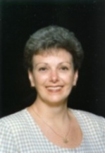
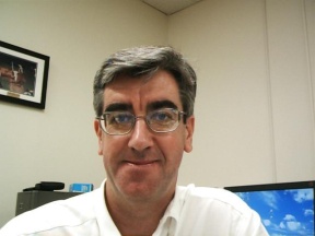
 Steve Pearton is a Professor of Materials Science and Engineering at the University of Florida. Prior to joining the university in 1994 he spent 10 years as a Member of Technical Staff at AT&T Bell Laboratories(now Lucent Technologies) in Murray Hill, NJ. He received his Ph.D. in physics from the University of Tasmania in Australia in 1983 and worked briefly at the Australian Atomic Energy Commission near Sydney prior to spending a year as a postdoctoral research associate at UC Berkeley and Lawrence Berkeley Laboratory. He is author or co-author of approximately 1300 journal articles, has given over 250 invited talks at international conferences, and has authored or edited 10 books. |
e-mail : pmath@mse.ufl.edu |
Current Members
 Jon Wright joined the group in 2005. He received his BS in MSE from The Ohio State University in 2005 and will gain an Masters from the University of Florida in Summer of 2007. His research focus concerns semiconductor processing for sensors, LEDs and UV detectors. Specifically, his studies center with Ohmic and Schottky contact formation, etching and ion implantation. |
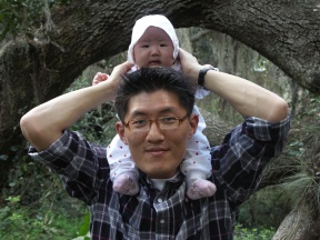 Wantae Lim received his BS in Electronic Engineering and his MS in Nano Engineering from Inje University in Korea in 2002 and 2005, respectively. He joined this group in Fall, 2005. His major research area is to develop etching mechanisms and Ohmic contact formation for oxide heterostructures. He is also studying on transparent thin film transistors(TFTs) for flexible display. |
Former Members
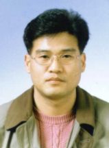 Hyun Cho was a postdoctoral research associate of Materials Science and Engineering at University of Florida. He received his Ph.D. in Inorganic Materials Engineering from Hanyang University in Korea in 1996, and spent his time at Ceramic Materials Research Institute (CMI) as a research associate prior to joining Professor Pearton’s research group in May, 1997. He is author or co-author of around 50 journal papers and a member of MRS and AVS. His current interests include developing of high density plasma and photoelectrochemical etch process for wide-bandgap semiconductor materials, especially III-nitrides, for fabrication of high power/high temperature electronics and short wavelength photonics. He is now a professor in Korea. |
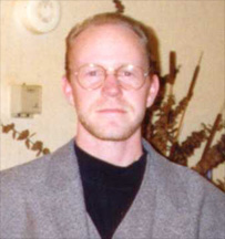 David Hays joined the Pearton research group in October, 1996 as an undergraduate research assistant. He investigated selective and non-selective wet etches for GaAs, AlGaAs, and InGaP. He also performed plasma damage studies and effects of hydrogenation in III-V’s. David received his Bachelor’s degree in Materials Science and Engineering from the University of Florida in May, 1998 and continued his research as a graduate student. His current research includes; developing selective dry etch chemistries for the GaAs/AlGaAs/InGaP and GaN/InN/AlN semiconductor systems, and developing high etch rate chemistries for Si MEMS processing. He will graduate in August, 1999 with a Masters degree in Materials Science and Engineering. He has authored more than 25 technical papers and 2 conference papers, and is a member of TMS, AVS, MRS, and ECS. He now works at GE Corporate R&D. |
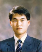 KeeBum Jung was a Ph. D. candidate of Materials Science and Engineering at the University of Florida. He received his M. S. degree in Electrical Engineering from the University of Florida in May 1996, and B. S. degree in Applied Physics from Inha University, Korea. His primary area of research is development of high density plasma etch processes for magnetic materials for magnetoresistive random access memory (MRAM) and giant magnetoresistive read/write head. He is an author or co-author of approximately 35 journal articles. He is a member of APS, AVS, MRS and TMS. He works for Applied Materials after completing a postdoc at IBM. |
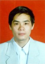 Xian-an Cao was a PhD student from China. He received his BS degree in Physics from Fudan University in Shanghai in 1995. After completion of his Master degree study in the Surface Physics Laboratory in Fudan, he joined this group in the fall, 1997. His research focused on implantation of GaN and related materials. His interests also cover other areas of semiconductor device processing, including wet and dry etching, rapid thermal annealing, contact, etc. He is a professor at the University of West Virginia after working at GE Corporate R&D. |
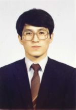 Who is Kyu-pil Lee (updated)? Kyu-pil Lee was born in Korea on May 28, 1961 and he is a Christian. He received his B.S. degree in Material Science and Engineering from Han Yang University in Seoul, Korea in 1985 and M.S degree in Material Science and Engineering from University of Florida in Gainesville, Florida in 2000. He joined the Semiconductor Research and Development Center of Samsung Electronics Co. in 1985. Since then he has worked as an architect for the development of CMOS technology and products, such as the 1Mb, 4Mb, 16Mb, 64Mb, 256Mb, 1Gbits, SOI-based CMOS memory devices and Low Voltage Battery Operation (LVBO) memory devices. In 1997, Samsung awarded him one of the best engineer to develop 1Giga-bit Dynamic Random Access Memory (1Gb DRAM) of the world’s first, and the excellent Patent Award for his R&D patent work for the Samsung. His publication is extensive and including a total of approximately over 35 journal papers and over 40 conference papers. Also he has received over 45 Korean patents, over 20 US, 12 Japanese, and several German, French, Italian and Taiwan patents for his original invention in the field. His credentials have earned him a place among the most influential individuals. Likewise, he listed in “Who’s Who in America” and ” Who’s Who in Science and Technologies ” and “Korean Biographical Dictionary” respectively. He joined the University of Florida for Ph.D. program according to the Samsung Human Resource Cultivation Program in 1998, and he is focusing on the development of Heterojunction Bipolar Transistor (HBT) using wide band gap materials. He is interested in Spintronic Devices using magnetic materials for the next generation memory devices |
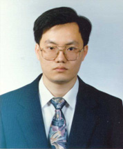 JeWon Lee was born in Seoul, Korea and received the B. S. degree in Inorganic Materials Engineering from the Hanyang University in Korea (1993). He then moved to the University of Florida, and received the M. S. and will be conferred the Ph. D. degree in the department of materials science and engineering in 1995 and 1997, respectively, under the guidance of Prof. Stephen J. Pearton. He spent his time in Sandia National Laboratories as a contract engineer, in Bell Laboratories, Lucent Technologies, Murray Hill, NJ as a visiting scientist, and in Samsung Electronics in Korea as a consultant in 1997. His research has covered a variety of areas in semiconductor device processing, including wet and dry etching, plasma enhanced chemical vapor deposition, ion implantation, surface degradation, device damage, hydrogen passivation, rapid thermal annealing and plasma process modeling. He has especially developed many plasma etching recipes for compound semiconductors, oxides, metals and flat panel displays with both Electron Cyclotron Resonance and Inductively Coupled Plasma sources, which has led to several awards to him as a graduate student. He is a member of ECS, AVS, MRS and TMS and an author of over 80 journal papers and 50 conference papers. He worked at Plasma-Therm Inc, St. Petersburg, FL in 1998 prior to joining a University in Korea. |
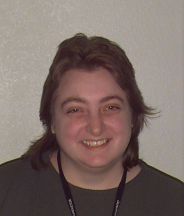 Cathy Vartuli received her Ph.D. in December 1996 for a thesis entitled “Development of Device Processing Techniques for III-Nitrides”. She is now employed at Lucent Technologies in Orlando FL, leading a group in the characterization area. |
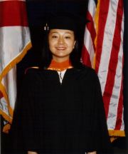 Juan-Juan Wang had joined Dr. Pearton’s research group in Summer, 1997 and received her Master and Ph.D. degrees in August 1998 and May 2002, respectively. She received her BS degree in Chemical Engineering from Chengdu University of Science and Technology in 1990, in China. She worked at Lucent prior to joining Northrop-Grumman. |
| Jin Hong received his Ph.D. in December 1998 for a thesis entitled “Inductively Coupled Plasma and Electron Cyclotron Resonance Plasma Etching of InGaAlP Compound Semiconductor System”. He is now employed at Samsung Semiconductor in Korea. | 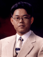 Kwang Baik received his Bachelor’s degree in Metallurgical Engineering Department at Yonsei University in Seoul, Korea in Fall 1998 and his Master degree in Materials Science and Engineering Department at the University of Florida in Spring 2002. His master thesis is titled “The Effect of Plasma Enhanced Chemical Vapor Deposition Passivation Layers on GaN.” He is pursuing his Ph.D. in UF Materials Science and Engineering. He works at SAIT in Korea. |
| Kelly Ip received her BS in Chemical Engineering and her MS in Materials Science and Engineering at the University of Florida in December 2000 and December 2002, respectively. She graduated in 2005 and worked at Intel prior to joining Raytheon. |
 Rohit Khanna received his BS in Ceramic Engineering from the Institute of Technology,Banaras Hindu University (IT-BHU),Varanasi,India in 2003. He joined the group in spring’04. His research area is semiconductor contact study & processing. He has to finish writing his dissertation, High Temp Contacts to GaN. He is also currently working as Assoc. Applications Engineer in Oerlikon, St. Petersburg and received his PhD at the end of summer’07. He is currently employed at Oerlikon in St. Petersburg, FL. |
 Lars Voss joined the group in 2004. He received his BS in Engineering Science from Penn State University in 2004 and his MS and PhD in Materials Science and Engineering from the University of Florida in 2007 and 2008. He is currently a postdoctoral researcher at Lawrence Livermore National Laboratories in Livermore, CA. |
